
Abstract
Thermal imaging has incredible medical device applications. Infrared light is the driving force behind this technology because it allows us to produce an image derived from temperature variations. Bolometers allow infrared light to be converted to temperatures and are produced through UV lithography. The final product is infrared sensors that are affordable and can be used for medical diagnostics. The range of applications is broad and exciting. Applications include disease detection and cancer therapeutics.
Introduction
On the outside, thermal imaging cameras don’t look much different from normal cameras, yet, on the inside, their functionality is radically different. Imagine if your baby monitor could tell you the temperature of your child without turning on the light, or if your doctor could see regions of skin cancer by taking your picture. These technologies are both possible because thermal imaging captures a different form of light: infrared.
Thermal imaging came to maturity through military applications, specifically advancements in night vision. Large contracts were awarded to the infrared industry during both the Gulf War and the War in Iraq5, which sparked many production advances. The technology then slowly migrated to the law enforcement arena3. It wasn’t until recently that thermal imaging has become an affordable option in new areas, such as the medical technology industry. The medical device field is ripe for an infrared revolution, whether it be improving early detection systems for certain diseases or advancing the latest therapeutic techniques. However, how does this kind of technology work?
Inner Workings of the Technology
Comprehension of the properties of infrared light is the key to understanding how these next-generation technologies can become a reality. It’s the fundamental concept behind how all thermal imaging cameras are able to measure temperatures.
Light is frequently categorized into six types or families. These families constitute what is called the full electromagnetic spectrum of light.8 Each individual family of light is made up of tiny packets of energy called photons. Within the visible light family–the kind of light our eyes see and normal cameras capture– different energies create the colors we see. The infrared light family also has different members based on energy differences. These types are called near-infrared light (high energy) and far-infrared light (low energy). Thermal imaging cameras only look at far-infrared light, because that is the kind of light that is emitted from all objects due to their temperature.
The temperatures of objects can be measured by the infrared light itself. This is important in the application of medical devices since non-invasive temperature measurement is the basis behind monitoring capabilities and cancer detection systems. The theory behind why objects emit infrared light when they have a higher temperature was first defined by Gustav Kirchhoff, a German physicist well known for his work on electrical circuits in the 1880s.14 He coined it the “Blackbody Effect,” and it remains the driving principle behind how each pixel in an infrared detector detects a temperature today.
Even though Kirchhoff’s principle is well known, the link behind the detection of infrared light and the reading of the temperature for medical applications is solved through a simple device called a bolometer. A bolometer is a special type of circuit that uses electrical resistance to measure temperature based on the amount and energy of infrared light that interacts with the circuit.
A common material used to produce these bolometers is vanadium oxide.15 Vanadium oxide intensely absorbs far-infrared light, which helps create a better image while still having the correct electrical properties required to read temperatures from the infrared measurement. A vanadium oxide bolometer is shown in Figure 1.

Figure 1: A vanadium oxide bolometer that converts infrared light into usable temperature readings for medical applications.
When placed in an array, a group of bolometers form an infrared sensor. This array can then collect temperature data and produce an image.
Lithography
Full infrared sensors are created using a technique called lithography. Lithography is a critical manufacturing technique through which silicon wafers are transformed into a final electronic device. Silicon is a naturally occurring element which is mined and refined into flat disks called wafers. When these wafers arrive, they come completely blank, ready for various electronic circuits to be painted on or carved into their surface. This versatility allows them to be carefully crafted to provide accurate medical diagnostics tools. The wafers are a chemical engineer’s blank palette, waiting for the paintbrush of lithography to transform them into beautifully engineered, microscopic pieces of art.
There are many kinds of lithographic production methods, but the most important and relevant technique is called UV (ultraviolet) lithography. This technique uses reactions just like the ones used when you get a filling cured at the dentist, to mask and print electronics on a silicon wafer. There are three main steps in the creation of a thermal imaging sensor: masking, deposition/sputtering, and lift off. Let’s walk through the infrared detector fabrication process using painting as an analogy10:
Masking: The first step is to mask off areas where we don’t want paint. In lithography, one way of masking is done by only shining UV light onto the surface of the wafer we don’t want to paint to go. UV light is used for this step because the surface of the wafer is usually coated with certain chemicals that rapidly harden with exposure to UV light, as if they got a permanent sunburn. The non-hardened chemicals then get washed away to make way for the next step, leaving behind the basic pattern for our circuit design.
Deposition/Sputtering (Painting): The second step is to paint on the first layer of colors. In infrared sensor production, the paint used is vaporized metals. While vaporized metals may sound strange, at extremely high temperatures, metals too can turn from solid to liquid to vapor. These vaporized metals are “spray painted” over the entire wafer surface and left to harden. Since we’ve already masked off the portions we don’t want to get painted the metal only gets deposited in the areas designated from before.
Lift Off (Let’s see the design!): Once the paint has dried, we can remove the tape to see the result of our fabrication. In microelectronics, this step is called lift off, because the hardened areas of chemicals from the masking step are removed so we can see the new structure we’ve created on top of the wafer surface.
These three basic steps provide the foundation for complex structures to be built, such as the processor inside your phone and PC or an infrared imaging sensor. In industry, these 3 steps are carefully performed and repeated over and over to achieve the desired results.
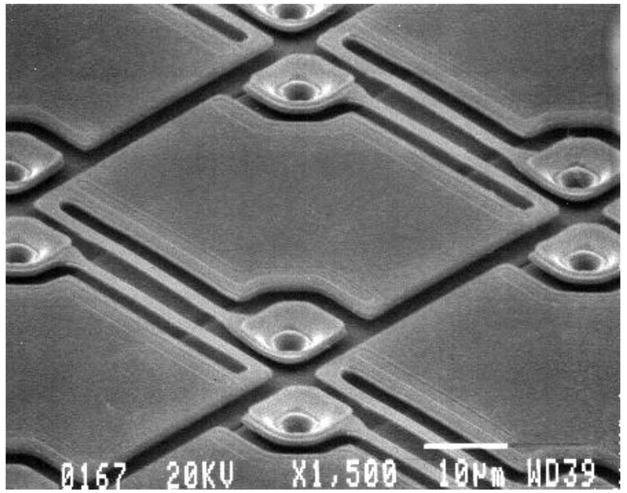
To finish creating an infrared sensor’s unique 3-D structure, infrared sensor production will sometimes employ another advanced step called etching. This technique uses special chemicals to give the sensor physical texture by carving valleys, creating mountains or forming bridges. It’s the step that gives the painter the tools to become a sculptor in case the need arises. In infrared sensor manufacturing, it has been discovered that 3-D structures far outperform their 2-D counterparts. Companies throughout the infrared industry compete over these proprietary sensor designs that attempt to push the boundaries of accurate measurement and quality.
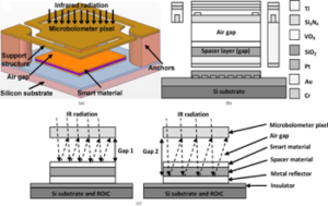
Figure 2: An example of a fully formed infrared sensor. Hundreds of these packed in a grid form thermal images we see [10].
Moore’s Law
Large increases in sensor quality and dramatic decreases in production cost due to advances in fabrication can be attributed to Moore’s Law. Moore’s Law was proposed in 1965 and states that every year, the size of microelectronic devices should be reduced by half.11 This is the same principle that has driven personal computer and smartphone microelectronics to the advances we see today.
Moore’s Law is strongly driven by engineering economics. Investments in increasingly advanced manufacturing techniques has consistently provided more than abundant returns on the investment. This concept is nicely summarized in Figure 3.
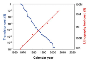
Figure 3: A plot showing the decreasing cost of microelectronics vs the increased cost of the tooling required [11].
Medical device applications are an exciting area for infrared advancement that hasn’t been fully explored. While many only dream about thermal cameras being embedded in self-driving cars that allow them to detect objects from a distance, next-generation thermal imaging technology has already been used to identify Ebola patients, showing how flexible and mature the technology has become.
Applications for Disease Detection
Thermometers are a great example of how thermal imaging could easily transform the way we care for children. What if you could use a thermal camera to visualize and measure a baby’s temperature, the temperature of their food, or their bath water? In addition to embedding thermal imaging cameras into a baby monitor to make sure they do not overheat, the cameras could also easily track their movements without having to turn on the lights.
Imagine a world where thermal imaging could be used to monitor patients or areas of the body for temperature changes that send an early signal that an infection may be beginning. Infections are very common complications to many surgeries, and early detection can be key to the success of a treatment.
Another application could be in the cleaning of medical devices. Medical devices often need to be sterilized at specific temperatures to kill bacteria and other pathogens. Monitoring the device to ensure every surface reaches the correct temperature in the autoclave may bring a huge advantage to identifying how pathogens could be spread through a hospital.
Applications for Advanced Therapeutics
One of the more advanced, actively researched applications is the use of infrared active therapeutic techniques to kill cancer cells. In these techniques, specifically designed nanoparticles are delivered to the cancer cell which collect infrared radiation to kill the unhealthy cells. This procedure could be improved with thermal imaging because it could allow the doctor to see the procedure in real-time to ensure the treatment is affecting the correct cells or targeting the correct area of the body.4 This could greatly increase the effectiveness of this emerging technique and decrease the number of treatments required to non-surgically remove and destroy certain types of cancer at an early stage.
The emerging economic and technological impact thermal imaging has on new areas of application makes this an exciting time. With so few applications thoroughly explored, especially in the medical device arena, there is room for thermal imaging to quickly become a subtle part of our everyday lives.
References
[1] A.Dutta, R. Sengupta, A. Krishnan, S. Islam, P. S. Wijewarnasuriya, and N. Dhar, “Broadband Image Sensors For Biomedical Security And Automotive Applications,” Proc. SPIE: International Society Optical Engineers, vol. 6769, p. 67690C.
[2] A. K. Sood, E. J. Egerton, Y. R. Puri, G. Fernandes, J. H. Kim, J. Xu, N. Goldsman, N. K. Dhar, P. S. Wijewarnasuriya, and B. I. Lineberry, “Carbon Nanotube Based Microbolometer Development For IR Imager and Sensor Applications,” Proc. SPIE 8155, Infrared Sensors, Devices, and Applications; and Single Photon Imaging II, vol. 8155, pp. 815513-815513–10, 2011.
[3] B. D. Figler, “Microbolometer uncooled thermal imaging sensors for law enforcement applications,” Proc. SPIE: Enabling Technologies for Law Enforcement and Security, vol. 4232, pp. 195–205, 2001.
[4] B.Nogrady, “Deep In The Red: Using Infrared To Watch What Goes On In A Living Body,” Scientific American, 2016. [Online]. Available: http://www.scientificamerican.com/article/fluorescent-tagging-living-body-tsien/. Accessed: Aug. 31, 2016.
[5] D. K. Breakfield and D. Plemons, “The Application of Microbolometers in 360° Ground Vehicle Situational Awareness,” Proc. SPIE: Infrared Technology and Applications XXXV, vol. 7298, p. 72981K–72981K–9, 2009.
[6] D. Z.-Y. Ting, S. V. Bandara, C. J. Hill, S. D. Gunapala, Y.-C. Chang, H. C. Liu, C. Y. Song, A. Soibel, J. Mumolo, J. Nguyen, J. K. Liu, S. A. Keo, S. B. Rafol, and E. R. Blazejewski, “Novel Quantum Well, Quantum Dot, and Superlattice Heterostructure Based Infrared Detectors,” Proc SPIE: Infrared Technology and Applications XXXV, vol. 7298, pp. 729805-729805–15, 2009
[8]”Electromagnetic spectrum,”. [Online]. Available: http://www.cyberphysics.co.uk/topics/light/emspect.htm. Accessed: Sep. 12, 2016.
[9] K. M. Palmer, “EUV Faces Its Most Critical Test,” IEEE Spectrum: Technology, Engineering, and Science News, 2011. [Online]. Available: http://spectrum.ieee.org/semiconductors/devices/euv-faces-its-most-critical-test. Accessed: Aug. 31, 2016.
[10] Qi Cheng, Suzanne Paradis, Truc Bui, and Mahmoud Almasri, “Design of Dual-Band Uncooled Infrared Microbolometer,” IEEE Sensors Journal, vol. 11, no. 1, pp. 167–175, Jan. 2011.
[11] S. E. Thompson and S. Parthasarathy, “Moore’s Law: The Future of Si Microelectronics,” MaterialsToday, vol. 9, no. 6, pp. 20–25, Jun. 2006.
[12] S. Landis, Ed., Nano Lithography. London: Wiley-ISTE, 2013.
[13] T. B. Breen, N. R. Butler, M. Kohin, C. A. Marshall, R. Murphy, T. W. Parker, and R. J. Silva, “Applications of Uncooled Microbolometer Sensors,” Proc. SPIE: Infrared Detectors and Focal Plane Arrays V, vol. 3379, pp. 145–156, 1998.
[14] T. London, Edinburgh, D. P. Magazine, and J. of Science, The London, Edinburgh and Dublin philosophical magazine and journal of science. Google Books, 1860. [Online]. Available: https://books.google.com/books?id=RVYEAAAAYAAJ&pg=PA1&lpg=PA1#v=onepage&q&f=false. Accessed: Sep. 12, 2016.
[15] Woo-Bin Song and Joseph J Talghader, “Design and characterization of adaptive microbolometers,” Journal of Micromechanics and Microengineering, vol. 16, no. 5, p. 1073, 2006.