At the time of writing, Kenneth Newton was a senior graduating with a B.S. in Electrical Engineering from the University of Southern California. He will be continuing his education at the University of Southern California as a Ph.D. student in the Electrophysics Department of Electrical Engineering.
The digital image sensor is a technology used to record electronic images. The most commonly recognized application of the digital image sensor is the digital camera. In digital cameras, the image sensor is used in conjunction with a color separation device and signal processing circuitry to record images. The two main technologies used to fabricate the sensors are CCD (Charge Coupled Device) and CMOS (Complimentary Metal-Oxide Semiconductor), each bearing certain advantages and disadvantages. Applications of the digital image sensor, including the pill camera and vision in robotics, are rapidly expanding, and soon sensors will be an everyday occurrence.
Introduction
The digital image sensor is a technology used to record electronic images. These image sensors are silicon microchips that are engineered to operate in different ways. The engineering involved in these circuits is very complex and the techniques used to manufacture these devices are not standardized in the industry. It is impractical to discuss the entire spectrum of manufacturing processes here, but they are noted because they give rise to the wide variety of applications for the digital image sensor. These engineering practices involve creating features that are added to the bare sensor for use in specific applications ranging from machine vision in robotics, to cameras integrated into cellular phones and PDAs, to ultraviolet sensors on the Hubble Space Telescope.
The most commonly recognized application of the digital image sensor is the digital camera. To get a sense of how image sensors are integrated in this application, their use in digital cameras will be explored. This exploration will also include an explanation of some of the other major features of a digital camera, as one must having a working knowledge of the lens and the mechanism for determining color in order to fully understand the role of the digital image sensor. One important thing to note about digital image sensors is that they are not all manufactured through the same processes. The two main technologies used to fabricate the sensors are CCD(Charge Coupled Device) and CMOS (Complimentary Metal-Oxide Semiconductor), which have certain key differences particularly in terms of performance, cost, and size.
The digital camera is not the only application of the image sensor. Another interesting application that has just recently become possible is the pill camera, which is a camera that can be swallowed and take pictures of the inside of the intestinal tract. As the technology used in the sensors progresses, there should be a multitude of exciting possible uses for the digital image sensor.
Digital Camera Technology
The most common application of the digital image sensor is the digital camera. In order to better understand the integration of the sensor into the camera, some of the external components used in the camera will be explained. The key components of the digital camera are the lens, which focuses light onto the image sensor, and the image sensor, which is used to replace conventional film. Image sensors used in digital cameras have special features, the most important of which is the ability to detect color. Currently three technologies are available to perform this function: a beam splitter, a spinning disk filter, and a color filter array.
The Lens
The lens is probably the chief similarity between the way digital cameras and conventional cameras work. The lens is the portal through which the image of the outside world reaches the image sensor. It focuses the light from the scene onto the sensor. The lenses used in digital cameras obey the exact same physics as lenses used in traditional cameras. Light from the subject passes through the lens and is focused on the film. The lens is chosen appropriately based on this principle so that the entire sensor is illuminated by the light. By moving the lens away from the film, the image of the subject is magnified, and only a portion of this magnified image appears on the film. The part of the image that appears on the film is a zoomed-in portion of the object, meaning this movement of the lens is the mechanism by which optical zoom works.
The Image Sensor
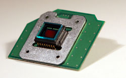
The basis of camera technology is a light-sensitive material that can reproduce an image (see Fig. 1). In a conventional camera the film is composed of Silver-Halide crystals suspended in gelatin — the same gelatin that Jell-O is made from [1]. In digital cameras this material is silicon, the same material used to make other electronics such as microprocessors. Silicon is a solid-state semiconductor that is refined from normal sand. Since its operation does not rely on a chemical reaction as conventional film does, a digital image sensor can be used repeatedly.
Converting Light to Electricity
The secret behind the workings of silicon film is converting light to electricity. When light strikes the surface of a piece of silicon, electrons, the smallest units of electric charge, are released. This happens because light transfers some or all of its energy to any electron it collides with. The number of free electrons is proportional to the amount of light that strikes the sensor, so the number of free electrons is proportional to the brightness of the scene.
In order to recreate an image, the sensor is broken down into a grid of millions of photosites. Each photosite makes up one portion of the picture called a picture element or pixel. Each photosite is exposed to only a small portion of the image, the portion of the image that comes from the corresponding area of the scene. The information from each individual block in the grid is pieced together to form a picture. As the number of photosites (squares in the grid) increases, the image created more closely resembles the subject. Readout of the image is done by special circuitry that counts the number of electrons at each photosite. Once the data is read in the form of electrical charge it is returned to its original state and can be used again.
Detecting Color
By itself, Silicon does not discern between colors — it simply detects the total amount of light that hits the surface. Without any alteration, a sensor would only be suited for taking black and white pictures. Special techniques must be used in order to produce color images. The color detection in these devices is achieved by only allowing specific wavelengths to pass through and expose the photosites. If a single photosite is only exposed to one color of light, then the readout from the photosite can be interpreted as color information.
The task of color separation is fairly simple because only three colors of light are required to reproduce natural color. By overlapping different combinations of red, blue, and green, any color in the visible spectrum can be reproduced. For example, when combining red and blue colors, the resulting color is purple. In the same way, by combining varying degrees of the three primary colors, any color can be reproduced.
The isolation of pixels to only one of these colors at a time is done by placing something that acts as a filter between the lens and the image sensor to separate the colors. There are three techniques to go about the color separation in different ways: a beam splitter, a rotating color filter, and a color filter array.
Beam Splitter
In the beam splitter implementation, light passes through a prism and is split into its three primary color components. Each of the primary colors is then projected onto separate sensors. We can easily observe this phenomenon by shining white light through a prism and noticing that the light coming out of the other side is split into its color components. The three primary colors are each diverted to a separate but identical sensor. Each sensor is exactly the same size and shape as the others and is positioned so that one of the three color components of the same image shows up on each one [1]. This means that for every pixel, there are three photosites: one per color. Signal processing circuitry then combines the information from the three sensors to create the final image.
This method creates a very high quality and accurate image because all of the necessary information is available in each pixel. The major drawback of this design is that three times as much sensor area is necessary since all three colors are captured separately. The cost of the extra sensors coupled with the need for a beam splitter results in a larger and more expensive camera.
Spinning Disk Filter
The spinning disk filter method is less complex than beam splitting. This method, just as it sounds, involves a plastic or metal disk that has three colored light filters positioned inside of it. By rotating the disk, one of the three filters is behind the lens at a time so that only one color can pass through. Each time a picture is taken the disk is rotated around so that each of the three colors is allowed to pass once. After the sensor is exposed to one color the data must be read off the sensor before it can be exposed to the next color, otherwise no special color information is obtained.
In this method, just like the last, every pixel is exposed to each color so the color quality is very good. Here, though, one sensor can be used instead of three, resulting in a lower cost. The big disadvantage of this technology is that it is not very good for taking pictures of moving objects. In the amount of time it takes for the filter to spin around once and read in all three colors, the subject may have moved and the image from each color will show the subject in a different position in space. When the images are overlapped there will be the appearance of a colored blur trailing any moving objects. Because of this cameras using spinning disk filters are better for still photography. It is also for this reason that we do not commonly see spinning disk filters used in cameras that are sold commercially.
Color Filter Array (CFA)
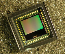
The color filter array is the most commonly used method in commercial digital camera applications. The CFA looks like a checkerboard with three colors instead of two (see Fig. 2). Each square of the checkerboard sits exactly over one pixel so that only one light color can pass through. Since our eyes are most sensitive to green, the popular pattern, called the Bayer pattern, allows more green light to pass through than red light or blue light. If the pattern is not properly aligned, the device will not work properly. Since each pixel is only exposed to one color, the signal processing for this method is more complicated than in the other methods. In other implementations the entire image is captured separately in each color which gives more exact coloration to the picture, but with CFA each pixel is dedicated to only one color. The CFA method still produces color well enough that the human eye does not notice a diminished color quality. In any given square of four pixels, all the colors are detected. The likelihood of color information changing brightness in large amounts for any two points next to each other is small, so data from nearby pixels can be reasonably factored in to create an accurate picture.
The CFA method saves cost and area without losing performance for high speed photography. It does, however, add the need for more complex algorithms of determining the color of the image created. These algorithms take into account the information of each photosite as well as the information of different colored photosites adjacent to it to determine the final color output for each pixel. These complex algorithms must be implemented by circuitry that also takes up space, but it is not nearly as much space as the physical mechanisms used in the spinning disk filter method or the beam splitting method.
Implementing a Sensor
In the current marketplace there are two main implementations of image sensors: CCD and CMOS. Both still rely on silicon as the “film,” but differ in the way they deal with the digital data and its processing. Each of these implementations has unique advantages and disadvantages.
CCD
CCD works much like a line of buckets where the water in each bucket gets poured into the next bucket. At the end of the line would be a large measuring cup that tells us how much water has been poured in from the last bucket. This information is then recorded and the water keeps moving down the chain until the amount of water in each bucket is recorded (see Fig. 3).
In the case of CCD technology we are pouring charge instead of water into the next pixel. This is done one row at a time by carrying out the identical process in parallel. The measuring bucket is an analog-to-digital converter that measures the amount of charge in each spot and then converts that amount to a number [2]. Once the data is converted to a number it is sent to a microprocessor to analyze and recreate the picture. The CCD fabrication process has been around for 50 years, so it has been engineered to the point where devices have excellent functionality. The process can typically involve up to 40 steps to create the pixels, the color filter arrays, and the other electrical features of the image sensors. However, the equipment used in the manufacturing process can only be used to create CCD devices, which by themselves do not have many applications aside from the image sensor. This means that the image processing circuitry has to be done on a separate chip, which can not be fabricated on the same machine, forcing most CCD manufacturers to purchase the image processing chip from an outside source. The CDD fabrication equipment is also very expensive because it only has a limited market; equipment manufacturers have to make their profit on individual unit sales instead of volume. Another pitfall of this technology is power consumption. It takes a lot of power to shift the charge from row to row, and as sensors are becoming more refined, the power consumption is increasing. This makes CCD technology unsuited for portable applications that only have a battery power supply [3].
CMOS
The CMOS process that has only recently been used to produce image sensors is the same technology that is used to create the image processing circuitry. Because of this, it is possible to integrate the image sensor and the image processing circuitry onto the same physical device.
In the passive pixel CMOS implementation the signal is not amplified and is instead read directly. In the active pixel CMOS image sensor implementation there are a number of transistors, between three and five depending on the application, that reside in the pixel. These transistors are there to amplify the signal to be read as well as help select which signals to read. With active pixel CMOS, pixels can be read one row, one column, or even one pixel at a time by the integrated image processing circuitry. Since there is no need to shift electrons, the power consumption of these devices is reduced significantly.
The most important thing about CMOS implementations of image sensors is the process used to make the devices. Since the image sensor and image processing circuit are made with the same process, light detection and signal processing can be done on the same chip. A big advantage of this process is that it takes fewer fabrication steps, between 20 and 30, to produce a device. The reduction in total number of steps makes the production faster and cheaper [4].
CMOS sensors are relatively new on the market, as they have only become popular in the past ten years, and the technology is still in a developmental stage. Because they are so new, CMOS sensors have some quality and resolutions issues compared with CCD, but engineers are working hard to improve them.
The Pill Camera
One application of the image sensor that is particularly interesting is the pill camera. The pill is swallowed and still images are taken every 30 seconds of the inside of the intestinal tract. The images are transmitted to a pack that clips on to the belt of the patient. This method of viewing a person’s intestinal tract is far less intrusive than the other popular method of sticking a fiber optic tube down a patient’s throat. After the camera has passed through the intestinal tract it stops taking pictures and can be disposed of. The implementation of this technology owes its existence to the reduced power consumption of CMOS. Using as little as one percent as much power as CCD devices, the CMOS image sensors can take about one hundred times as many pictures as a CCD sensor with the same battery supply.
Studies have shown that this technology is able to diagnose cases of gastrointestinal bleeding that the fiber optic method misses. Patients also prefer this method as it is much less intrusive and uncomfortable [5].
The Possibilities
The presence of image sensors in everyday objects is already a reality and there is no indication that the industry will stop growing. The CCD market has been around for a long time, and CMOS image sensors are a hot new technology that will allow for even wider use of image sensors. Image sensors have already found a limited role in medical fields, and this role will certainly expand in the future. Other specialized uses of image sensors that exist today are in machine vision, where robots can have the capability to recognize and manipulate objects. As this field grows, image sensors may play an important part in allowing robotic systems to interact more directly with human beings. The possibility of cameras being included in every electronic device that has any circuitry at all becomes more reasonable as the technology gets smaller and cheaper. Imagine a camera in a toaster that helps you decide if the toast is done. This may seem like a ridiculous use for the technology, but it is merely an example of how commonplace image sensors may be in our lives in the years to come.
References
-
- [1] K. Nice and G.J. Gurevich. “How Digital Cameras Work.” Howstuffworks. Internet: http://electronics.howstuffworks.com/digital-camera.htm, Feb. 2003.
- [2] S. A. Campbell. “The Science and Engineering of Microelectronic Fabrication. Second edition.” New York: Oxford University Press, 2001.
- [3] B.S. Hur and M.G. Kang. “High definition color interpolation scheme for progressive scan CCD image sensor.” IEEE Transactions on Consumer Electronics, vol. 47, pp. 179-186, 2001.
- [4] Micron Imaging. Internet: http://www.micron.com/imaging/, Feb. 2003.
- [5] P.A. Tipler. “Physics. Fourth edition.” New York: W.H. Freeman and company, 1999.